sexta-feira, 16 de setembro de 2011

Criando o Copper Pour

Voltamos novamente com o layout, mas agora é a parte de acabamento final.
Primeiramente vamos arrumar os textos em silk screen (SST), com a Text Tool selecionada, devemos remover os nomes desnecessários e adotar um padrão de disposição, por exemplo somente à direita e  em cima, salvo algumas exceções  em que não é possível posicionar nos devidos nichos.
Agora vamos adicionar uma camada de preenchimento de cobre, associada à malha do terra, para prover proteção caso haja algo em curto este será aterrado, além disso serve também para filtrar possíveis ruídos. Assim com Obstacle Tool faça um retângulo na placa toda e clique na borda selecionando New, em Obstacle Type selecione Copper pour, em Width e Clearance coloque 0.5 e em Net Attachment marque 0 (GND), clique em OK.


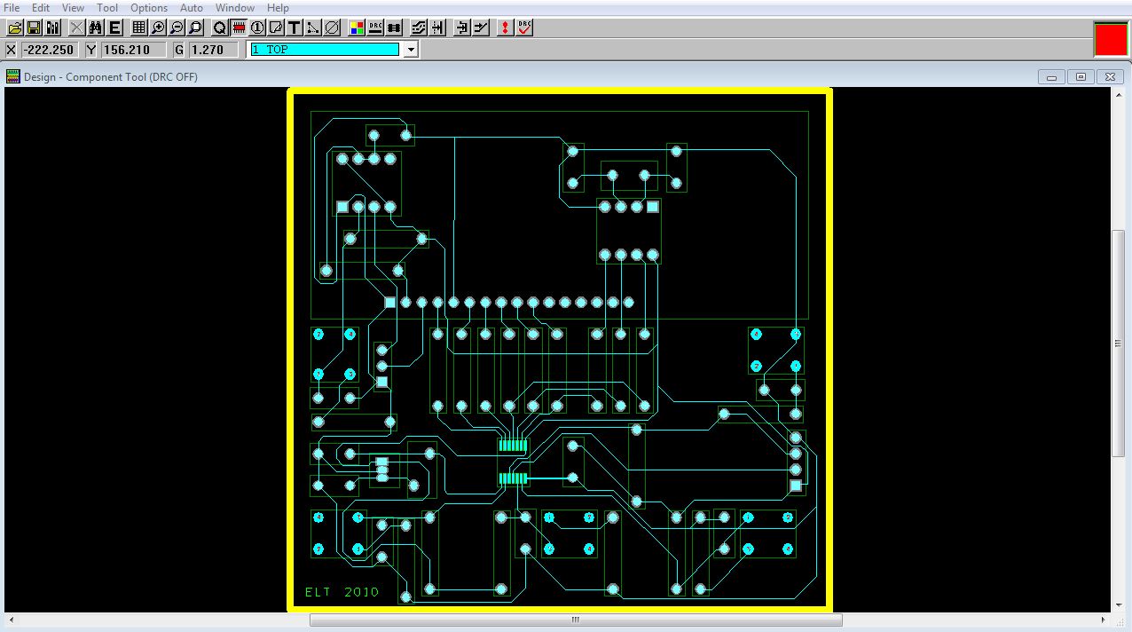
O programa irá renderizar o preenchimento e sobrepor todas as linhas de terra, conectando-se aos pads por pequenos filamentos apenas. Então a aparência do layout deverá ser essa:


No post seguinte, mostraremos como gerar e visualizar o gerber do nosso layout para o projeto do relógio com o MSP430-F2013.

sexta-feira, 9 de setembro de 2011

Routing the board


Continuing the confection of the layout we will now move on to the Board routing the MSP430-F2013.
First, we must create a barrier that will limit the area of the plate with Obstacle Tool. Now let's position the components with Component Tool, as a convenience for the best routing, watching the links so that there is less junction of routes. If you do not have patience to make a hard manual work and want to automatically route, you must first go into OPTIONS, Route Strategies, Route Layers and disable all icons with the Botom. Will now have to go in AUTO, Autoroute, Board. Otherwise click the button "add/edit mode" and draw the trails starting from part of signup, after feeding. Remember that automatic routing is a quick solution for routing only, it is strongly recommended to do manually for the the better use of space.
If you're hardcore and will do it manually start by developing digital signal extends from MSP and after passing to the analog. Finally do the routing of Vcc and GND, remembering that if you reach a point where spare some vi to be linked, but it is not possible to do without crossing other tracks, you can add a jumper, just add a resistor 0Ω in the Schematic Capture.
To update the layout where there has been some change in the schematic, one should keep open the Layout Plus and the Capture, this should go on Create Netlist and select "Run ECO", returning to this layout should ask to update automatically.
To add a footprint created an existing component you must right-click on the component with the Component Tool button and select Properties and then Footprint in new tab choose the desired footprint.


Then we should have a layout as below:


sexta-feira, 2 de setembro de 2011

Roteamento de placa

Continuando a confecção do layout vamos agora passar para o roteamento da placa do MSP430-F2013.
Primeiramente, devemos criar um obstáculo que limitará a área da placa, com Obstacle Tool. Agora vamos posicionar os componentes com Component Tool, conforme a conveniência para o melhor roteamento, prestando atenção nas ligações para que haja menos cruzamento de vias. Se você não tiver paciência de fazer um árduo trabalho manual e quiser rotear automaticamente, deve-se primeiramente ir em OPTIONS, Route Strategies, Route Layers e desabilitar todos ícones com Botom.  Agora terá que ir em AUTO, Autoroute, Board. Caso contrário clicar no botão “add/edit mode” e desenhar as trilhas começando pela parte de sinal, depois a alimentação. Lembrar que o roteamento automático é uma solução rápida apenas para o roteamento, é fortemente recomendado fazer manualmente para o melhor aproveitamento de espaço.
Se você é hardcore e vai fazer manualmente comece pelas vias de sinal digital partindo do MSP e depois passando para o analógico. Por fim faça o roteamento do Vcc e do GND, lembrando que se você chegar num ponto onde sobra alguma vi a ser ligada, mas não seja possível fazer sem cruzar outras trilhas, poderá adicionar um jumper, basta adicionar um resistor de 0Ω no esquemático do Capture.
Para atualizar o layout caso tenha havido alguma mudança no esquemático, deve-se manter aberto o Layout Plus e o Capture, neste mesmo deve-se ir em Create Netlist e selecionar “Run ECO”, voltando ao layout este deve pedir para atualizar automaticamente.
Para adicionar um footprint criado a um componente já existente deve-se clicar com o botão direito no componente com o botão Component Tool e selecionar Properties e depois Footprint, na nova aba escolher a footprint desejada.
Então deveremos ter um layout como o abaixo:


No próximo episódio continuaremos no layout, por hoje é tudo pessoal.


sexta-feira, 26 de agosto de 2011

Creating land patterns


After making the schematic, several times, we will for the first part of the layout, construction and the use of footprints.
With all connected components, click the main file (.DSN), go on TOOLS, Create Netlist, Select User properties are in milimeters. Should then generate a netlist file with the same name as the schema.
To open the Layout, go on TOOLS, Library Manager, another screen appears, click Add in the Libraries, go to the folder (C:) where Orcad and search is installed in the folder (\Layout_Plus\Library) the file METRIC.LLB.
To make a new footprint for the components in the Library Manager, you must click Create New Footprint, now just add the pads (TOOLS, Padstack) according to data from the datasheet of the component, filling only those fields marked as TOP and add DRILL measure if they are True Hole. To obstacle click (Obstacle Tool) check the format of borders and right click on them, selecting Properties and then selecting Place Outline and Global Layer to make the component format in silk screen is the same, but you must select Detail and SSTOP.


For a com component libraries already known, in time to make the link must seek the most appropriate according to the dimensions in the datasheet. For example a component Dip of 8 legs true hole the corresponding library is DIP100T, and the footprint is the DIP. 100/300/8/w. L.400, W the width and L the length.


Returning to the Layout, go to FILE, New, go to the folder of Orcad on (C:) and search (\Layout_Plus\Data) the file METRIC.TCH then must search the previously generated netlist "Nome.MNL", in the same directory as the schematic.
Most components will find footprint ready, however the MSP, LCD and Switch we should do our own footprints as described in the datasheet of the component.
If the program asks to find a footprint for a component, not cited oil, one should look for some template as the table.


Component
Footprint
LM555
DIP.100/8/W.300/L.425
HT1380
DIP.100/8/W.300/L.400
LM35
TO92
Resistor
AX/RC07
Capacitor
RAD/.300X.125/LS.200/.031
Indutor
DISC/.350X.175/LS.200X.100/.034
Potenciômetro
SIP/TM/L.300/3

sexta-feira, 19 de agosto de 2011

Criando footprints para o layout

Após fazer o esquemático, várias vezes, passaremos para primeira parte do layout, a contrução e o uso de footprints.
Com todos os componentes conectados, clicar no arquivo principal (.dsn), ir em TOOLS, Create Netlist,  selecionar User properties are in milimeters. Deverá então gerar um arquivo de netlist com o mesmo nome do esquemático.
Ao abrir o Layout, ir em TOOLS, Library Manager, aparecerá outra tela, no Libraries clicar em Add, ir até a pasta em (C:) onde está instalado o Orcad e procurar na pasta (\Layout_Plus\Library) o arquivo METRIC.LLB.
Para fazer um novo footprint para os componentes no Library Manager, deverá clicar em Create New Footprint, agora é só adicionar os pads (TOOLS, Padstack) de acordo com os dados do datasheet do componente, preenchendo apenas os campos marcados como TOP e adicionar medida de DRILL se forem True Hole. Para obstáculo clicar em (Obstacle Tool) marcar o formato das fronteiras e clicar com a direita neles, selecionando Properties e em seguida marcando Place Outline e Global Layer, para fazer o formato do componente em silk screen é o mesmo, mas deve-se selecionar Detail e SSTOP.

Tabela de padstack do MSP430-F2013:

Para um componente com bibliotecas já conhecidas, na hora de fazer o link deve-se procurar a mais apropriada de acordo com as dimensões no datasheet. Por exemplo um componente Dip de 8 pernas true hole a biblioteca correspondente será DIP100T, e o footprint adequado é o DIP.100/8/W.300/L.400, sendo W a largura e L o comprimento.

A Footprint do MSP é conforme a imagem:

Voltando ao Layout, ir em FILE, New, ir até a pasta do Orcad em (C:) e procurar em (\Layout_Plus\Data) o arquivo METRIC.TCH, em seguida deverá procurar o netlist gerado anteriormente “Nome.MNL”, no mesmo diretório do esquemático.
A maioria dos componentes irá encontrar footprint pronto, entretanto o MSP, LCD e Switch deveremos fazer nossos próprio footprints de acordo com o descrito no datasheet do componente.
Caso o programa peça para encontrar algum footprint para um componente, não citados àcima, deve-se procurar algum modelo conforme a tabela.

Tabela de footprints prontas:
Componente
Footprint
LM555
DIP.100/8/W.300/L.425
HT1380
DIP.100/8/W.300/L.400
LM35
TO92
Resistor
AX/RC07
Capacitor
RAD/.300X.125/LS.200/.031
Indutor
DISC/.350X.175/LS.200X.100/.034
Potenciômetro
SIP/TM/L.300/3


No post seguinte continuaremos com a criação do layout para o projeto.

sexta-feira, 12 de agosto de 2011

Schematics V2.0


Hi, in this post we will do a review of our clock project with the MSP430-F2013, before leaving for the layout. As you can see in electronics projects are made and remade, until they reach the required capacity, so we will have multiple versions of Alpha, Beta ...
Let's start by reviewing the problem of consumption, first observe that the largest expense lcd backlight came from, so we should turn it and only connect when it is pressed a button to check the time. For this we will use a 555 to function as timer and turn off the led lcd, this because the micro ports are crowded, so cannot resolve the problem in hardware, software only on its mounting was configured as the datasheet. Second, another expense that will be cut off is of LM7805, so rather than use a 9V battery will use a 5V which has generally 2000mAh. Now in this way we will have increased to lifetime of approximately 7 months clock.
Other changes required for the project is the addition of resistors in the communication of lcd and HT1380 to the MSP. This increase is necessary due to the potential difference between the micro and the components are 5V in the instant communication, there is some barrier to current is extremely high, so there must be binding on resistors. An appropriate value for the resistors for the lcd 47 kΩ is and for the HT is 1 k ohms.
For connection to LM35 will do a filter "pi" is a low pass filter to eliminate multiple frequency oscillator, with two capacitors and one inductor as noted in this second version of the schematic.


Now our schematic is ready and we can go to the layout in the next post.
See ya!


sexta-feira, 5 de agosto de 2011

Esquemático V2.0 do projeto

Olá, neste post faremos uma revisão do nosso projeto de relógio com o MSP430-F2013, antes de partir para o layout. Como é possível notar na eletrônica os projetos são feitos e refeitos, até atingirem a capacidade exigida, por isso teremos várias versões do relógio alfa, beta...
Vamos começar revendo o problema de consumo, primeiro observamos que o maior gasto vinha da backlight do lcd, portanto devemos desliga-la e apenas ligar quando for pressionado um botão para checar a hora. Para isso iremos usar um 555 para funcionar como temporizador e desligar o led do lcd, isto pois as portas do micro estão lotadas, logo não podemos resolver o problema em software apenas em hardware, sua montagem foi configurada conforme o datasheet. Segundo, outro gasto que será cortado é do LM7805, assim ao invés de usarmos uma bateria de 9V usaremos uma de 5V que tem em geral 2000mAh. Agora dessa maneira teremos a vida útil do relógio acrescida para aproximadamente 7 meses.
Outra alteração necessária para o projeto é a adição de resistores na comunicação do lcd e HT1380 ao MSP. Esse acréscimo é necessário devido à diferença de potencial entre o micro e os componentes serem de 5V no instante de comunicação, não havendo alguma barreira a corrente é altíssima, portanto é preciso haver resistores na ligação. Um valor apropriado para os resistores para o lcd é de 47KΩ e para o HT é de 1KΩ.
Para ligação ao LM35 iremos fazer um filtro “pi” é um filtro passa baixa para eliminar frequências múltiplas do oscilador, com dois capacitores e um indutor conforme nota-se nessa segunda versão do esquemático.


Agora sim nosso esquemático está pronto e poderemos passar ao layout no próximo post.