sexta-feira, 30 de setembro de 2011

Gerando e visualizando o gerber

Olá caros seguidores, hoje para finalizar nosso layout do relógio com o MSP430-F2013 iremos criar o gerber, grupo de arquivos que são enviados para a empresa que confeccionará o circuito impresso.
Primeiramente vá em Options, Post Process Settings nessa janela clique nas linhas de todas as opções com bottom e na nova janela desmarque a opção “Enable for post processing”, deixe essa opção marcada apenas para (TOP, SMT, SST, AST, DRD). Feito isso vá em Auto e clique em Run Post Processor, o Orcad agora deve criar no diretório do arquivo aberto vários arquivos de gerber como (nome.TOP, .SST, .SMT, .GTD, . DRD, .AST, .lis, .DTS e TRUEHOLE.tap)


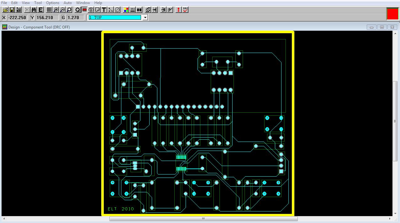
Para visualizarmos o gerber como será impresso temos que usar algum programa, no caso usaremos o Viewplot, que é gratuito e pode ser encontrado aqui.
Abrindo o programa, carregue o arquivo gerado “nome.TOP”, e aparecerá algo como:


Pronto agora passamos por toda parte de projeto e especificação de hardware, criação do esquemático e layout. Temos então um projeto a meio caminho andado.

sexta-feira, 23 de setembro de 2011

Creating the copper pour


We return again with the layout, but now is part of the final finishing.
First let's get the texts at silk screen (OSH), with the Text Tool selected, we should remove the unnecessary names and adopt a pattern of provision, for example only to the right and upon, except a few exceptions in that you cannot place in appropriate niches.
Now let's add a fill layer copper, associated with the mesh of the Earth, to provide protection in case there is something in short this is grounded, in addition it also serves to filter out possible noise. So with Obstacle Tool make a rectangle on the entire plate and click on the edge by selecting New in Obstacle Type select Copper pour, in Width and Clearance put 0.5 and Net Attachment select 0 (GND), click OK.


The program will render the fill and superimpose all land lines, connecting the pads by small filaments only. Then the appearance of the layout should be this:


In the next post, we'll show you how to generate and view the gerber of our layout to the design of the clock with the MSP430-F2013.

sexta-feira, 16 de setembro de 2011

Criando o Copper Pour

Voltamos novamente com o layout, mas agora é a parte de acabamento final.
Primeiramente vamos arrumar os textos em silk screen (SST), com a Text Tool selecionada, devemos remover os nomes desnecessários e adotar um padrão de disposição, por exemplo somente à direita e  em cima, salvo algumas exceções  em que não é possível posicionar nos devidos nichos.
Agora vamos adicionar uma camada de preenchimento de cobre, associada à malha do terra, para prover proteção caso haja algo em curto este será aterrado, além disso serve também para filtrar possíveis ruídos. Assim com Obstacle Tool faça um retângulo na placa toda e clique na borda selecionando New, em Obstacle Type selecione Copper pour, em Width e Clearance coloque 0.5 e em Net Attachment marque 0 (GND), clique em OK.


O programa irá renderizar o preenchimento e sobrepor todas as linhas de terra, conectando-se aos pads por pequenos filamentos apenas. Então a aparência do layout deverá ser essa:


No post seguinte, mostraremos como gerar e visualizar o gerber do nosso layout para o projeto do relógio com o MSP430-F2013.

sexta-feira, 9 de setembro de 2011

Routing the board


Continuing the confection of the layout we will now move on to the Board routing the MSP430-F2013.
First, we must create a barrier that will limit the area of the plate with Obstacle Tool. Now let's position the components with Component Tool, as a convenience for the best routing, watching the links so that there is less junction of routes. If you do not have patience to make a hard manual work and want to automatically route, you must first go into OPTIONS, Route Strategies, Route Layers and disable all icons with the Botom. Will now have to go in AUTO, Autoroute, Board. Otherwise click the button "add/edit mode" and draw the trails starting from part of signup, after feeding. Remember that automatic routing is a quick solution for routing only, it is strongly recommended to do manually for the the better use of space.
If you're hardcore and will do it manually start by developing digital signal extends from MSP and after passing to the analog. Finally do the routing of Vcc and GND, remembering that if you reach a point where spare some vi to be linked, but it is not possible to do without crossing other tracks, you can add a jumper, just add a resistor in the Schematic Capture.
To update the layout where there has been some change in the schematic, one should keep open the Layout Plus and the Capture, this should go on Create Netlist and select "Run ECO", returning to this layout should ask to update automatically.
To add a footprint created an existing component you must right-click on the component with the Component Tool button and select Properties and then Footprint in new tab choose the desired footprint.


Then we should have a layout as below:


sexta-feira, 2 de setembro de 2011

Roteamento de placa

Continuando a confecção do layout vamos agora passar para o roteamento da placa do MSP430-F2013.
Primeiramente, devemos criar um obstáculo que limitará a área da placa, com Obstacle Tool. Agora vamos posicionar os componentes com Component Tool, conforme a conveniência para o melhor roteamento, prestando atenção nas ligações para que haja menos cruzamento de vias. Se você não tiver paciência de fazer um árduo trabalho manual e quiser rotear automaticamente, deve-se primeiramente ir em OPTIONS, Route Strategies, Route Layers e desabilitar todos ícones com Botom.  Agora terá que ir em AUTO, Autoroute, Board. Caso contrário clicar no botão “add/edit mode” e desenhar as trilhas começando pela parte de sinal, depois a alimentação. Lembrar que o roteamento automático é uma solução rápida apenas para o roteamento, é fortemente recomendado fazer manualmente para o melhor aproveitamento de espaço.
Se você é hardcore e vai fazer manualmente comece pelas vias de sinal digital partindo do MSP e depois passando para o analógico. Por fim faça o roteamento do Vcc e do GND, lembrando que se você chegar num ponto onde sobra alguma vi a ser ligada, mas não seja possível fazer sem cruzar outras trilhas, poderá adicionar um jumper, basta adicionar um resistor de 0Ω no esquemático do Capture.
Para atualizar o layout caso tenha havido alguma mudança no esquemático, deve-se manter aberto o Layout Plus e o Capture, neste mesmo deve-se ir em Create Netlist e selecionar “Run ECO”, voltando ao layout este deve pedir para atualizar automaticamente.
Para adicionar um footprint criado a um componente já existente deve-se clicar com o botão direito no componente com o botão Component Tool e selecionar Properties e depois Footprint, na nova aba escolher a footprint desejada.
Então deveremos ter um layout como o abaixo:


No próximo episódio continuaremos no layout, por hoje é tudo pessoal.